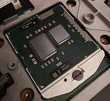
 The mobile Core i7-640M. The large die (on the left) is the CPU component and the small die (on the right) is the iGPU | |
| General information | |
|---|---|
| Launched | 2010 |
| Marketed by | Intel |
| Designed by | Intel |
| Common manufacturer(s) | |
| Product code | 80617 |
| Performance | |
| Max. CPU clock rate | 1.06 GHz to 2.66 GHz |
| Cache | |
| L1 cache | 128 KB (64 KB (32 KB instructions + 32 KB data) per core) |
| L2 cache | 512 KB (256 KB per core) |
| L3 cache | Up to 4 MB |
| Architecture and classification | |
| Application | Dual-core mobile |
| Technology node | 32 nm |
| Microarchitecture | Westmere |
| Instruction set | x86, x86-64, MMX, SSE, SSE2, SSE3, SSSE3, SSE4.1, SSE4.2, AES-NI |
| Physical specifications | |
| Cores |
|
| Memory (RAM) |
|
| GPU(s) | Intel HD Graphics |
| Socket(s) |
|
| Products, models, variants | |
| Brand name(s) | |
| History | |
| Predecessor(s) | Penryn |
| Successor(s) | Sandy Bridge |
| Support status | |
| Unsupported | |
Arrandale is the code name for a family of mobile Intel processors, sold as mobile Intel Core i3, i5 and i7 as well as Celeron and Pentium.[1][2] It is closely related to the desktop Clarkdale processor; both use dual-core dies based on the Westmere 32 nm die shrink of the Nehalem microarchitecture, and have integrated Graphics as well as PCI Express and DMI links.
Arrandale is the successor of the 45 nm Core-microarchitecture-based Penryn processor that is used in many of the mobile Core 2, Celeron and Pentium Dual-Core processors. While Penryn typically used both a north bridge and a south bridge, Arrandale already contains the major northbridge components, which are the memory controller, PCI Express bus for external graphics, integrated graphics, and the DMI interface, making it possible to build more compact systems.
The Arrandale processor package contains two dies: the 32 nm processor die with the I/O connections, and the 45 nm Intel HD Graphics (Ironlake) controller and integrated memory controller die.[3] Physical separation of the processor die and memory controller die resulted in increased memory latency.
Arrandale was released on 7 January 2010, during CES 2010.[4]
Brand names
Arrandale processors were sold under the Celeron, Pentium, Intel Core i3, Intel Core i5 and Intel Core i7 brand names, with only the Core i7 models using the full L3 cache and all features. Processors ending in E instead of M are embedded versions with support for PCIe bifurcation and ECC memory, while the regular mobile versions only support a single PCIe port and non-ECC memory. The Celeron versions of Arrandale have the smallest L3 cache of just 2 MB.[5]
| Brand Name | Model (list) | L3 Cache size | Thermal Design Power |
|---|---|---|---|
| Intel Celeron | P4xxx | 2 MB | 35 W |
| U3xxx | 18 W | ||
| Intel Pentium | P6xxx | 3 MB | 35 W |
| U5xxx | 18 W | ||
| Intel Core i3 | i3-3xxM | 3 MB | 35 W |
| i3-3xxUM | 18 W | ||
| Intel Core i5 | i5-4xxM, i5-5xxM, i5-5xxE | 3 MB | 35 W |
| i5-4xxUM, i5-5xxUM | 18 W | ||
| Intel Core i7 | i7-6xxM, i7-6xxE | 4 MB | 35 W |
| i7-6xxLM, i7-6xxLE | 25 W | ||
| i7-6xxUM, i7-6xxUE | 18 W |
See also
- Consumer Ultra-Low Voltage (CULV) computing platform
- List of Macintosh models grouped by CPU type
References
- ↑ Anton Shilov. "Intel May Unveil Microprocessors with Integrated Graphics Cores at Consumer Electronics Show". Archived from the original on 2010-10-30. Retrieved 2009-09-27.
- ↑ Intel to launch four Arrandale CPUs for mainstream notebooks in January 2010. Digitimes.com (2009-11-13). Retrieved on 2011-06-15.
- ↑ The Delayed Mobile Nehalems: Clarksfield, Arrandale, and the Calpella Platform. Brighthub.com (2009-02-22). Retrieved on 2011-06-15.
- ↑ Intel Arrandale: 32nm for Notebooks, Core i5 540M Reviewed. AnandTech. Retrieved on 2011-06-15.
- ↑ "Products formerly Arrandale". Intel. Retrieved 2018-02-10.
Discontinued