| Computer memory and data storage types |
|---|
| Volatile |
| Non-volatile |
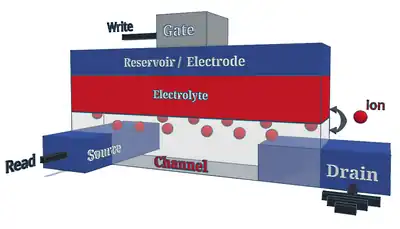
Electrochemical Random-Access Memory (ECRAM) is a type of non-volatile memory (NVM) with multiple levels per cell (MLC) designed for deep learning analog acceleration.[1][2][3] An ECRAM cell is a three-terminal device composed of a conductive channel, an insulating electrolyte, an ionic reservoir, and metal contacts. The resistance of the channel is modulated by ionic exchange at the interface between the channel and the electrolyte upon application of an electric field. The charge-transfer process allows both for state retention in the absence of applied power, and for programming of multiple distinct levels, both differentiating ECRAM operation from that of a field-effect transistor (FET). The write operation is deterministic and can result in symmetrical potentiation and depression, making ECRAM arrays attractive for acting as artificial synaptic weights in physical implementations of artificial neural networks (ANN). The technological challenges include open circuit potential (OCP) and semiconductor foundry compatibility associated with energy materials. Universities, government laboratories, and corporate research teams have contributed to the development of ECRAM for analog computing. Notably, Sandia National Laboratories designed a lithium-based cell inspired by solid-state battery materials,[4] Stanford University built an organic proton-based cell,[5] and International Business Machines (IBM) demonstrated in-memory selector-free parallel programming for a logistic regression task in an array of metal-oxide ECRAM designed for insertion in the back end of line (BEOL).[6] In 2022, researchers at Massachusetts Institute of Technology built an inorganic, CMOS-compatible protonic technology that achieved near-ideal modulation characteristics using nanosecond fast pulses [7]
Operation

Write
Stress to the gate, relative to channel electrodes, can be applied in the form of fixed current or bias, driving ions toward - or away from - the electrolyte/channel interface where charge transfer occurs with free carriers. Upon insertion in the channel, the ionic charge is neutralized and the atomic species intercalate or bind to the conductive host matrix, in some cases yielding strain and localized phase transformation. Such reversible processes are equivalent to anodic/cathodic reactions in battery cells or electrochromic devices. Although in ECRAM, the programming of the memory element is defined not as a change in capacity or opacity, but by a change of channel conductivity associated with atomic species being inserted or removed as a result of the stress signal.
Read
The read operation is decoupled from the write operation thanks to the presence of three electrodes, therefore limiting read disturb. A small bias is applied between the channel electrodes, with the resulting read current being proportional to the channel conductivity, hence sensing the programmed state of the device.
Speed
The programming speed of ECRAM cells is not limited by the bulk diffusion of ions. They indeed only need to cross the interface plane between the electrolyte and the channel to induce a change in conductivity. Nanosecond write pulses can indeed trigger programming.[8] Trade-offs between gate capacitance, electronic conductivity, etc., can yield settling transients, limiting the maximum read-write frequency.[9]
Arrays
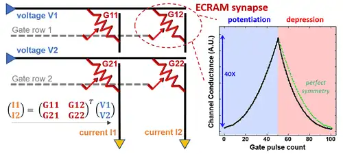
ECRAM arrays are integrated in a pseudo-crossbar layout, the gate access line being common to all devices in a row or column. If a change in electrochemical potential, the driving force of a battery, occurs upon ionic exchange between channel and gate electrode, an open circuit potential (OCP) exists at the gate contact and will differ device to device depending on the programmed state. To prevent cross-talk between cells sharing a gate line, an access device to isolate each one is added in series with the memory element.[10] Suppressing OCP in the ECRAM design, minimizes the cell size/complexity, allowing for selector-free parallel read/programming of device arrays.[6]
Synaptic function

Principle
Non-volatile memory (NVM) can be leveraged for in-memory compute, thereby reducing the frequency of data transfer between storage and processing units. This can ultimately improve compute time and energy efficiency over hierarchical system architectures by eliminating the Von Neumann bottleneck. Hence, when using multi-level cells (MLC) at the nodes of cross-bar arrays, one can perform analog operations on time or voltage encoded data such as vector (row input signal) × matrix (memory array) multiply. Following Kirchhoff's and Ohm's laws, the resulting vector is then obtained by integrating the current collected at each column. For ECRAM cells, an additional line is added at each row to write the cells during programming cycles, thereby yielding a pseudo-crossbar architecture. In the field of artificial intelligence (AI), deep neural networks (DNN) are used for classification and learning tasks, relying on a large number of matrix-multiply operations. Therefore, analog compute with NVM technology for such tasks are extremely attractive. ECRAM cells are uniquely positioned for use in analog deep learning accelerators due to their inherent deterministic and symmetric programming nature when compared to other devices such as resistive RAM (ReRAM or RRAM) and phase-change memory (PCM).
Requirements
| Metric | Unit | NVM synaptic cell target[11] |
|---|---|---|
| G range | nS | 9-72 |
| on/off ratio | n.a. | 8 |
| # of states | n.a. | 1000 |
| up/down asymmetry | % | 5 |
| write time | ns | 1 |
Physical implementation of artificial neural networks (ANN) must perform at iso-accuracy when benchmarked against floating point precision weights in software. This sets the boundary for device properties needed for analog deep learning accelerators. In the design of their resisistive processing unit (RPU), IBM Research has published such requirements,[11] a subset of which is listed here. Algorithm and hardware co-design can relax them somewhat but not without other trade-offs.[12]
NVM use as synaptic weights in lieu of storage implies significantly different requirements when it comes to target resistance range, number of levels, and programming speed and symmetry. Because the in-memory computation occurs in parallel through the array, many devices are addressed concurrently and therefore need to have a high average resistance to limit energy dissipation. To perform high-accuracy computation and be resilient to noise, the NVM cell needs a large number of distinct states. The programming time needs only to be fast between levels, not from the highest to the lowest resistance states. During each programming cycle (back-propagation), weight updates can be negative or positive, and the up/down traces therefore need symmetry to allow learning algorithms to converge. All NVM technologies do struggle with these targets. ECRAM individual cells can meet such stringent metrics,[6] but also need to demonstrate high-density array yield and stochasticity.
Demos with ECRAM Synaptic Arrays
Sandia National Laboratories
As reported in a 2019 publication in Science, by Elliot J. Fuller, Alec A. Talin, et al. from Sandia National Laboratories, in collaboration with Stanford University, and the University of Massachusetts Amherst:[10]
Using co-planar organic multilevel cells, isolated by conductive bridge memory (CBM) devices, the team demonstrates parallel programming and addressing in up to 3×3 arrays. In particular a 2-layer neural network is mapped to the array by transferring the weights necessary to perform an inference task resulting in a XOR operation on the binary input vector.
Individual cells are shown to have the following properties (not all achieved in the same device configuration); speed = 1 MHz read-write cycles, number of states > 50 (tunable), resistance range = 50-100 nS (tunable), endurance > 108 write ops, size = 50×50 μm2.
IBM Research
As reported in a 2019 proceeding of the IEEE International Electron Device Meeting (IEDM), by Seyoung Kim, John Rozen, et al. from IBM Research:[6]
Using metal-oxide ECRAM cells, selector-free, the team demonstrates parallel programming and addressing in 2×2 arrays. In particular, a logistic regression task is performed in-memory with 1,000 2×1 vectors as training set. 2D curve fit is achieved in a dozen epochs.
Individual cells are shown to have the following properties (not all achieved in the same device configuration); speed = 10 ns write pulses, number of states > 1,000 (tunable), resistance range = 0-50 μS (tunable), endurance > 107 write ops, size < 1×1 μm2.
Cell implementations
Various institutions have demonstrated ECRAM cells with vastly different materials, layouts, and performances.
An example set for discrete cells is listed in the table.
| Ion | Channel | Device Size | Write Pulse Length | Reference |
|---|---|---|---|---|
| Li+ | WO 3 | 100 x 100 nm2 | 5 ns | [8] |
| Li+ | Li 1−xCO 2 | ~1 mm2 | 0.5 s | [4] |
| Li+ | Graphene | 36 μm2 | 10 ms | [13] |
| Li+ | α-MO 3 | ~1 mm2 | 10 ms | [14] |
| H+ | PEDOT:PSS | 0.001 mm2 | 5 ms | [5] |
| H+ | WO 3 | 0.05 mm2 | 5 ms | [15] |
| H+ | WO 3 | 0.025 mm2 | 210 ms | [16] |
| H+ | WO 3 | 0.01 mm2 | 0.1 s | [17] |
| H+ | 2D MXene | 100 µm2 | 200 ns | [18] |
Li-ECRAM
Based on lithium ions, Li-ECRAM devices have demonstrated repeatable and controlled switching by applying known materials from battery technology to the memory design.[4][13][14] Consequently, such cells can exhibit an OCP which varies over several volts, depending on the programmed state.
H-ECRAM
Based on hydrogen ions, H-ECRAM devices have proven fast, necessitating small driving forces to induce programming.[5][15][16] High diffusion coefficients in various materials can be accompanied by lack of retention within the memory cell, impacting endurance. Most H-ECRAM designs use liquid and/or organic electrolytes. In a 2022 study, researchers at Massachusetts Institute of Technology demonstrated a CMOS-compatible technology based on phosphosilicate glass electrolyte that achieved ultrafast modulation characteristics with high energy efficiency.[7] The same year researchers at the Royal Institute of Technology KTH showed ECRAMS based on hydrogen intercalation into the 2D material MXene, marking the first demonstration of high speed 2D ECRAMs. [18]
MO-ECRAM
Metal-oxide based ECRAM, are inspired from OxRam materials and high-k/metal gate technology used in commercial semiconductor offerings. MO-ECRAM do enable negligible OCP and sub-μs write operations.[6]
VLSI

For advanced semiconductor memory or compute applications, a technology needs to be compatible with very large scale integration (VLSI). This puts constraints on materials used, and the techniques employed to fabricate functional devices. The implications for ECRAM are described here.
Semiconductor foundry
A semiconductor foundry can handle several technologies and has strict rules when it comes to materials being introduced in its expensive toolset to avoid cross-contamination and loss of device yield. In particular, metallic mobile ions, if present in active areas, can induce device drift and affect reliability. There are several other considerations for the foundries; including safety, cost, volume, etc. Hence, lithium ion-based Li-ECRAM faces unique challenges beyond the presence of OCP.
Back end of line (BEOL)
Memory arrays require logic periphery to operate and interface with the rest of the compute system. Such periphery is based on field-effect transistors (FETs) built on the surface of silicon wafer substrates with a high thermal budget at the front end of line (FEOL). Memory cells can be inserted between upper metal levels at back end of line (BEOL) but will still need to remain unaffected by temperatures up to ~400 °C used in subsequent steps. Together with high density patterning challenges, these restrictions make organic devices unsuitable for such integration. The ECRAMs based on 2D MXene materials [18] have shown the potential to be unaffected by 400 °C heating, but additional development is needed for the integration of ion conductors.
Heterogeneous integration (HI)
One way to introduce novel memory materials can be to use heterogeneous integration (HI) where the device array is fabricated independently from the logic controls and then bonded to the FET-containing chip to enable its use as high bandwidth memory (HBM). However, the cost and complexity associated with such scheme negatively affects the value proposition for displacing existing memory technologies.
References
- ↑ Shi, J.; Ha, S. D.; Zhou, Y.; Schoofs, F.; Ramanathan, S. (2013). "A correlated nickelate synaptic transistor". Nature Communications. 4: 2676. Bibcode:2013NatCo...4.2676S. doi:10.1038/ncomms3676. PMID 24177330.
- ↑ Tang, Jianshi; Bishop, Douglas; Kim, Seyoung; Copel, Matt; Gokmen, Tayfun; Todorov, Teodor; Shin, SangHoon; Lee, Ko-Tao; Solomon, Paul (2018-12-01). "ECRAM as Scalable Synaptic Cell for High-Speed, Low-Power Neuromorphic Computing". 2018 IEEE International Electron Devices Meeting (IEDM). pp. 13.1.1–4. doi:10.1109/IEDM.2018.8614551. ISBN 978-1-7281-1987-8. S2CID 58674536. Retrieved 2020-07-16.
- ↑ "Finite element modeling of electrochemical random access memory - iis-projects". iis-projects.ee.ethz.ch. Zürich, Switzerland: ETH Zurich. Retrieved 2020-07-16.
- 1 2 3 'E. J. Fuller et al., Adv. Mater., 29, 1604310 (2017)
- 1 2 3 Y. van de Burgt et al., Nature Electronics, 1, 386 (2018)
- 1 2 3 4 5 Kim, S. (2019). "Metal-oxide based, CMOS-compatible ECRAM for Deep Learning Accelerator". 2019 IEEE International Electron Devices Meeting (IEDM). pp. 35.7.1–4. doi:10.1109/IEDM19573.2019.8993463. ISBN 978-1-7281-4032-2. S2CID 211211273.
- 1 2 Onen, Murat; Emond, Nicolas; Wang, Baoming; Zhang, Difei; Ross, Frances M.; Li, Ju; Yildiz, Bilge; del Alamo, Jesús A. (29 July 2022). "Nanosecond protonic programmable resistors for analog deep learning". Science. 377 (6605): 539–543. doi:10.1126/science.abp8064. ISSN 0036-8075. PMID 35901152. S2CID 251159631.
- 1 2 Tang, J. (2018). "ECRAM as Scalable Synaptic Cell for High-Speed, Low-Power Neuromorphic Computing". 2018 IEEE International Electron Devices Meeting (IEDM). pp. 13.1.1–4. doi:10.1109/IEDM.2018.8614551. ISBN 978-1-7281-1987-8. S2CID 58674536.
- ↑ D. Bishop et al., proceedings of the international conference in Solid-State Devices and Materials (SSDM), pp. 23-24 (2018)
- 1 2 Fuller, E.J.; Keene, S.T.; Melianas, A.; Wang, Z.; Agarwal, S.; Li, Y.; Tuchman, Y.; James, C.D.; Marinella, M.J.; Yang, J.J.; Salleo, A.; Talin, A.A. (2019). "Parallel programming of an ionic floating-gate memory array for scalable neuromorphic computing". Science. 364 (6440): 570–4. Bibcode:2019Sci...364..570F. doi:10.1126/science.aaw5581. PMID 31023890. S2CID 133605392.
- 1 2 Tayfun, G.; Yurii, V. (2016). "Acceleration of Deep Neural Network Training with Resistive Cross-Point Devices: Design Considerations". Frontiers in Neuroscience. 10: 333. doi:10.3389/fnins.2016.00333. PMC 4954855. PMID 27493624.
- ↑ Tayfun, G.; Haensch, H. (2020). "Algorithm for Training Neural Networks on Resistive Device Arrays". Frontiers in Neuroscience. 14: 103. doi:10.3389/fnins.2020.00103. PMC 7054461. PMID 32174807.
- 1 2 Sharbati, M.T.; Du, Y.; Torres, J.; Ardolino, N.D.; Yun, M.; Xiong, F. (2018). "Artificial Synapses: Low-Power, Electrochemically Tunable Graphene Synapses for Neuromorphic Computing". Adv. Mater. 30: 1870273. doi:10.1002/adma.201870273.
- 1 2 Yang, C.-S.; Shang, D.-S.; Liu, N.; Fuller, E.J.; Agrawal, S.; Alec Talin, A.; Li, Y.-Q.; Shen, B.-G.; Sun, Y. (2018). "All-Solid-State Synaptic Transistor with Ultralow Conductance for Neuromorphic Computing". Adv. Funct. Mater. 28 (42): 1804170. doi:10.1002/adfm.201804170. OSTI 1472248. S2CID 104934211.
- 1 2 Yao, X.; Klyukin, K.; Lu, W. (2020). "Protonic solid-state electrochemical synapse for physical neural networks". Nat Commun. 11 (1): 3134. Bibcode:2020NatCo..11.3134Y. doi:10.1038/s41467-020-16866-6. PMC 7371700. PMID 32561717.
- 1 2 Yang, J.-T.; Ge, C.; Du, J.-Y.; Huang, H.-Y.; He, M.; Wang, C.; Lu, H.-B.; Yang, G.-Z.; Jin, K.-J. (2018). "Artificial Synapses Emulated by an Electrolyte-Gated Tungsten-Oxide Transistor". Adv. Mater. 30 (34): 1801548. doi:10.1002/adma.201801548. PMID 29974526. S2CID 49655665.
- ↑ J. Lee et al., proceedings of the IEEE international Silicon Nanoelectronics Workshop (SNW), pp. 31-32 (2018)
- 1 2 3 Melianas, Armantas; Kang, Min‐A; VahidMohammadi, Armin; Quill, Tyler James; Tian, Weiqian; Gogotsi, Yury; Salleo, Alberto; Hamedi, Mahiar Max (March 2022). "High‐Speed Ionic Synaptic Memory Based on 2D Titanium Carbide MXene". Advanced Functional Materials. 32 (12): 2109970. doi:10.1002/adfm.202109970. ISSN 1616-301X. S2CID 244484634.
External links
- Moore, S.K. (11 December 2018). "Searching for the Perfect Artificial Synapse for AI". IEEE Spectrum.
- Ambrogio, S.; Adusumilli, P.; Eleftheriou, E. (11 December 2019). "The path to the "perfect" analog material and system: IBM at IEDM and NeurIPS". IBM Research Blog.
- Chandler, D.L. (19 June 2020). "Engineers design a device that operates like a brain synapse". MIT News.
- Kubota, T. (25 April 2019). "Stanford researchers' artificial synapse is fast, efficient and durable". Stanford News.
- "Sandia Powers Breakthroughs in Neuromorphic Computing". inside HPC. 1 May 2019.