
The EnCore microprocessor family is a configurable and extendable implementation of a compact 32-bit RISC instruction set architecture - developed by the PASTA Research Group at the University of Edinburgh School of Informatics. The following are key features of the EnCore microprocessor family:
- 5 stage pipeline
- highest operating frequency in its class
- lowest possible dynamic energy consumption - 99% of flip-flops automatically clock-gated using typical synthesis tools
- most non-memory operations achieving single-cycle latency, and no more than one load-delay slot
- easy configurability of cache architectures
- compact baseline instruction set architecture (ISA), including freely-mixed 16-bit and 32-bit encodings for maximum code density
- no overhead for switching between 16- and 32-bit instruction encodings
All of the EnCore test chips are named after hills in Edinburgh; Calton, being the smallest, is the first of these. The second, Castle, is named after the rock on which Edinburgh Castle is built.
EnCore Calton
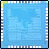
The first silicon implementation of the EnCore processor is a test-chip code-named Calton, fabricated in a generic 130nm CMOS process using a standard ASIC flow.
- 130nm implementation of EnCore processor in baseline configuration extended with barrel shifter, multiplier, and a full set of 32 general purpose registers.
- Contains bus interface and system control functions, in addition to the processor.
- Implemented with 8KB direct-mapped instruction- and data-cache.
- Complete system-on-chip occupies 1 mm2 of silicon at 75% utilization.
- Chip-level power consumption is 25 mW at 250 MHz.
- First silicon samples operate above a frequency of 375 MHz at typical voltage and temperature.
EnCore Castle
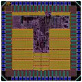
The second silicon implementation of an extended EnCore processor is a test-chip codenamed Castle, fabricated in a generic 90nm CMOS process.
The Castle chip contains an extended version of the EnCore processor, together with a 32KB 4-way set-associative Instruction Cache, and a 32KB 4-way set-associative Data Cache. It is embedded within a system-on-chip (SoC) design that provides a generic 32-bit memory interface, as well as interrupt, clocks and reset signals.
- 90nm implementation is based on a generic free foundry libraries, and a stack of 9 metal layers.
- Complete design occupies 2.25 sq.mm on a 1.875 x 1.875 mm die. This includes the baseline CPU, the reconfigurable Configurable Flow Accelerator (CFA) extension logic, two 32KB caches, and the off-chip interfaces.
- Designed to operate on a core voltage of 0.9V to 1.1V, with 2.5V LVCMOS I/O signals.
- Packaged in a 68-pin Ceramic LCC.
- First silicon samples operate at 600MHz.
- Chip-level power consumption is 70mW at 600 MHz, under typical conditions.
- Complete design flow, from RTL to GDSII, was performed by the PASTA team. This was based on an in-house developed design flow using Synopsys Design Compiler for topological synthesis, and IC Compiler for automated place-and-route.
- Over 97% of all flip-flops in the design were automatically clock-gated during logic synthesis.
- LVS and DRC checks were performed using Calibre, from Mentor Graphics.