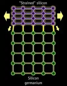
Strained silicon is a layer of silicon in which the silicon atoms are stretched beyond their normal interatomic distance.[1] This can be accomplished by putting the layer of silicon over a substrate of silicon–germanium (SiGe). As the atoms in the silicon layer align with the atoms of the underlying silicon germanium layer (which are arranged a little farther apart, with respect to those of a bulk silicon crystal), the links between the silicon atoms become stretched - thereby leading to strained silicon. Moving these silicon atoms farther apart reduces the atomic forces that interfere with the movement of electrons through the transistors and thus better mobility, resulting in better chip performance and lower energy consumption. These electrons can move 70% faster allowing strained silicon transistors to switch 35% faster.
More recent advances include deposition of strained silicon using metalorganic vapor-phase epitaxy (MOVPE) with metalorganics as starting sources, e.g. silicon sources (silane and dichlorosilane) and germanium sources (germane, germanium tetrachloride, and isobutylgermane).
More recent methods of inducing strain include doping the source and drain with lattice mismatched atoms such as germanium and carbon.[2] Germanium doping of up to 20% in the P-channel MOSFET source and drain causes uniaxial compressive strain in the channel, increasing hole mobility. Carbon doping as low as 0.25% in the N-channel MOSFET source and drain causes uniaxial tensile strain in the channel, increasing electron mobility. Covering the NMOS transistor with a highly stressed silicon nitride layer is another way to create uniaxial tensile strain. As opposed to wafer-level methods of inducing strain on the channel layer prior to MOSFET fabrication, the aforementioned methods use strain induced during the MOSFET fabrication itself to alter the carrier mobility in the transistor channel.
History
The idea of using germanium to strain silicon for the purpose of improving field-effect transistors appears to go back at least as far as 1991.[3]
In 2000, an MIT report investigated theoretical and experimental hole mobility in SiGe heterostructure-based PMOS devices.[4]
In 2003, IBM was reported to be among primary proponents of the technology.[5]
In 2002, Intel had featured strained silicon technology in its 90nm X86 Pentium microprocessors series in early 2000.[5] In 2005 Intel was sued by AmberWave company for alleged patent infringement related to strained silicon technology.
See also
References
- ↑ Sun, Y.; Thompson, S. E.; Nishida, T. (2007). "Physics of strain effects in semiconductors and metal–oxide–semiconductor field-effect transistors". Journal of Applied Physics. 101 (10): 104503–104503–22. Bibcode:2007JAP...101j4503S. doi:10.1063/1.2730561. ISSN 0021-8979.
- ↑ Bedell, S.W.; Khakifirooz, A.; Sadana, D.K. (2014). "Strain scaling for CMOS". MRS Bulletin. 39 (2): 131–137. doi:10.1557/mrs.2014.5. ISSN 0883-7694.
- ↑ Vogelsang, T.; Hofmann, K.R. (November 1992). "Electron mobilities and high-field drift velocities in strained silicon on silicon-germanium substrates". IEEE Transactions on Electron Devices. 39 (11): 2641–2642. doi:10.1109/16.163490.
- ↑ E. Tanasa, Corina (September 2002). Hole Mobility and Effective Mass in SiGe Heterostructure-Based PMOS Devices (Report). Massachusetts Institute of Technology.
- 1 2 Lammers, David (2002-08-13). "Intel adopts strained silicon for 90-nanometer process". EDN. Retrieved 2022-07-09.
External links
- Development of New Germanium Precursors for SiGe Epitaxy; Presentation at 210th ECS Meeting (SiGe Symposium), Cancun, Mexico, October 29, 2006.
- Safer alternative liquid germanium precursors for relaxed graded SiGe layers and strained silicon by MOVPE; Deo V. Shenai, Ronald L. DiCarlo, Michael B. Power, Artashes Amamchyan, Randall J. Goyette and Egbert Woelk; Journal of Crystal Growth, Volume 298, Pages 172-175, January 7, 2007.