Atomic Terrace Low Angle Shadowing (ATLAS) is a surface science technique which enables the growth of planar nanowire or nanodot arrays using molecular beam epitaxy on a vicinal surface. ATLAS utilises the inherent step-and-terrace structure of the surface as a template for such nanostructures.[1][2] The technique involves the low angle incidence of flux material on vicinal substrates. Vicinal substrates are composed of atomic terraces separated by atomic steps. The ATLAS technique allows for the fabrication of well defined planar arrays of plasmonic nanostructures, of dimensions unachievable by lithography.
A collimated beam of atoms or molecules is evaporated at an oblique angle to the substrate. This causes the steps to "shadow" the beam, and the molecules to be adsorbed only on the exposed parts of the steps in direct line of sight of the evaporator.
The principal attraction of the technique is its relative simplicity, as it does not involve multiple lithography steps and can be applied to metal, semiconductor or oxide surfaces alike.
The technique is a "bottom-up" approach and allows great control over the separation of nanostructures within the array, as well as their individual widths. The separation is controlled by the size of the atomic terraces of the substrate, which is determined by its miscut from the principal index; and the width of the nanostructures is controlled by the oblique angle of the deposition.
ATLAS has been shown to be a very versatile technique, with the growth of metallic, semi-conducting and magnetic nanowires and nanodots demonstrated using a variety of source materials and substrates.[3]
Basic Principles

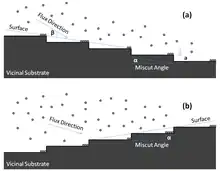
Figure 1(a) shows a schematic of the deposition in the "downhill" direction, that is, from an outer step edge to a lower terrace. The deposition angle β between the beam and surface is small (1°-3°) so that some areas of the terraces are exposed to the beam, and others are geometrically shadowed.
The deposition angle β determines the width of the nanostructures, according to the following relation:
where w is the nanostructure width, a is the height of one step, α is the miscut angle and β is the deposition angle between the incident beam and the surface (α and β are assumed to be small and are measured in radians).
Figure 1(b) shows a similar situation, but this time with the substrate rotated by 180° so that the incident beam is now in the "uphill" direction, and nearly parallel to the surface. In this case, the step faces provide the bonding sites and the deposited material grows along the steps, similar to the step-flow growth mechanism.
In order to grow nanowires with a width of fifteen nanometers or less, the deposition temperature for both orientations should be chosen such that the mean free path of the adatoms on the surface is limited to a few nanometers.
Experimental Development
The ATLAS system was developed within the Applied Physics Group at the School of Physics, Trinity College, Dublin. The experimental procedure is relatively straightforward, when compared to lithography or other approaches, meaning that only standard equipment is needed.
The set-up consists of an ultrahigh vacuum chamber (base pressure in the low 10−10 Torr range), with the sample mounted at a large working distance (40-100 cm) from the evaporation source. This large distance provides the high collimation required for the ATLAS technique. The sample itself is mounted on a rotation stage and can be tilted through 200° with a precision of ±0.5°.
The substrate can be heated during deposition by either passing direct current through the sample for semiconductors or by driving current through a separate heating foil underneath the substrate for insulating oxides.
Versatility
The capabilities of the system were first tested by growing arrays of 10-30 nm wide metallic nanowires on two types of vicinal substrates, step-bunched Si(111) and α-Al2O3(0001). Deposition of Au and Ag onto these substrates yields arrays of wires with a width and height of 15 nm and 2 nm, and separated by approximately 30 nm.
Since its introduction in 2008, ATLAS has been demonstrated as a simple technique to produce nanowires of a variety of materials down to a width of 15 nm and thickness of 2 nm, on several stepped substrates.
Limitations
Although ATLAS is a versatile technique, some limitations do exist. The initial growth of the nanowires is nucleated on certain preferential adsorption sites. This can form epitaxial seeds, which grow independently of each other, until they meet, which forms an overall polycrystalline wire. This polycrystallinity can affect the stability of the wire when exposed to air, and can increase the resistance due to its defective nature. It is an ongoing topic of research to increase the quality of nanowires by lattice matching, or increasing initial mobility through heating of the substrate.
Despite these limitations, ATLAS's results of a 15 nm width is approximately a five-fold reduction in size compared to other shallow-angle techniques.[4]
References
- ↑ F. Cuccureddu, V. Usov, S. Murphy, C. O. Coileain, I. V. Shvets, Planar nanowire arrays formed by atomic-terrace low-angle shadowing, Rev. Sci. Instrum. 79, 053907 (2008), Archived 2014-04-09 at archive.today
- ↑ Cuccureddu, F.; Usov, V.; Murphy, S.; Coileain, C.O.; Shvets, I. (20 May 2008). "Planar nanowire arrays formed by atomic-terrace low-angle shadowing". Review of Scientific Instruments. 79 (5): 053907–053907–4. Bibcode:2008RScI...79e3907C. doi:10.1063/1.2929835. hdl:2262/40319. ISSN 0034-6748. PMID 18513079.
- ↑ Floriano Cuccureddu, Shane Murphy, Igor V. Shvets, Mauro Porcu, H. W. Zandbergen, Plasmon Resonance in Silver Nanoparticles Arrays Grown by Atomic Terrace Low-Angle Shadowing, Nano Lett., 2008, 8 (10), pp 3248–3256,
- ↑ J. Oster, M. Kallmayer, L. Wiehl, H. J. Elmers, H. Adrian, F. Porrati, M. Huth, J. Appl. Phys. 97, 014303 (2005),