A gap surface plasmon (or gap plasmon) is a guided electromagnetic wave which propagates in a transparent medium located between two extremely close metallic regions. Propagating in a gap between metals forces light to propagate partially inside the metallic regions,[1] causing the gap plasmon to slow down.
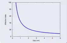
The velocity of the gap-plasmon can be modulated by changing the thickness of the gap even by a few nanometers.

A gap-plasmon is a guided mode, a solution of Maxwell's equations without source. It is the form under which light propagates inside an extremely thin gap between two metals (having the same nature or not). As a gap plasmon, the electromagnetic wave can propagate up to four to five times slower than in vacuum. Such a guided mode only exists for parallel to the interface magnetic fields (p polarization). The distance between the metallic area has to be typically smaller than 50 nm in order to noticeably slow the guided mode. Actually, the GAP plasmon propagates partially inside the metal : the field of the GAP plasmon penetrates the metal to a depth of typically 25 nm, called the skin depth. A slow guided mode presents a short effective wavelength and so a very large wave vector (noted kx when the wave propagates along an Ox axis). As the thickness of the dielectric region decreases, the gap-plasmon is slowed by the metal and its effective index (as well as its wavevector) increases, while its effective wavelength shrinks.
Devices based on gap-plasmon, such as resonators, present a typical size which is of the order of the effective wavelength. Gap-plasmon resonators have in general a reduced size compared to the wavelength of light in vacuum. Such a miniaturization is particularly sought after in plasmonics.
Applications
- Gap plasmon resonators :

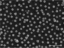
They can be obtained by self-assembly of chemically synthesized nanocubes or by lithography. A GAP plasmon resonator is a cavity for the guided mode : the wave is reflected back and forth inside the resonator.
Such structures (see picture) present a very small volume compared to the wavelength is vacuum (which allow to reach a very important Purcell effect). Such resonators can then be used to design metasurfaces, fabricate reflection holograms or for subwavelength color printing.
Example : chemically synthesized silver nanocubes on a gold layer, separated by polymer (see picture).
- Electro-optical modulators[2] :
Electro-optical modulators are designed to modulate a light signal, i.e. they modulate on the characteristics of a light beam (such as its wavelength, polarization state or intensity) to encode a signal. The gap plasmon based modulators are the smallest existing modulators.[3] Losses are reduced thanks to this small size. They operate over a large frequency range. Actually, the upper frequency limit of such devices is currently beyond the reach of electronic measuring devices.
References
- ↑ Rabih, Ajib (April 2019). "The energy point of view in plasmonics" (PDF). Journal of the Optical Society of America B. 36 (4): 1150. arXiv:1904.02607. Bibcode:2019JOSAB..36.1150A. doi:10.1364/JOSAB.36.001150. S2CID 102353260.
- ↑ "Electro-optic modulator", Wikipedia, 2021-11-13, retrieved 2021-12-14
- ↑ Haffner, Christian; Heni, Wolfgang; Fedoryshyn, Yuriy; Josten, Arne; Baeuerle, Benedikt; Hoessbacher, Claudia; Salamin, Yannick; Koch, Ueli; Đorđević, Nikola; Mousel, Pol; Bonjour, Romain (December 2016). "Plasmonic Organic Hybrid Modulators—Scaling Highest Speed Photonics to the Microscale". Proceedings of the IEEE. 104 (12): 2362–2379. doi:10.1109/JPROC.2016.2547990. hdl:20.500.11850/117058. ISSN 1558-2256. S2CID 7139146.