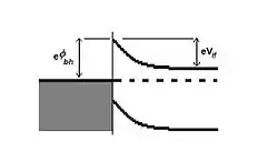
In bulk semiconductor band structure calculations, it is assumed that the crystal lattice (which features a periodic potential due to the atomic structure) of the material is infinite. When the finite size of a crystal is taken into account, the wavefunctions of electrons are altered and states that are forbidden within the bulk semiconductor gap are allowed at the surface. Similarly, when a metal is deposited onto a semiconductor (by thermal evaporation, for example), the wavefunction of an electron in the semiconductor must match that of an electron in the metal at the interface. Since the Fermi levels of the two materials must match at the interface, there exists gap states that decay deeper into the semiconductor.
Band-bending at the metal-semiconductor interface
As mentioned above, when a metal is deposited onto a semiconductor, even when the metal film as small as a single atomic layer, the Fermi levels of the metal and semiconductor must match. This pins the Fermi level in the semiconductor to a position in the bulk gap. Shown to the right is a diagram of band-bending interfaces between two different metals (high and low work functions) and two different semiconductors (n-type and p-type).
Volker Heine was one of the first to estimate the length of the tail end of metal electron states extending into the semiconductor's energy gap. He calculated the variation in surface state energy by matching wavefunctions of a free-electron metal to gapped states in an undoped semiconductor, showing that in most cases the position of the surface state energy is quite stable regardless of the metal used.[2]
Branching point
It is somewhat crude to suggest that the metal-induced gap states (MIGS) are tail ends of metal states that leak into the semiconductor. Since the mid-gap states do exist within some depth of the semiconductor, they must be a mixture (a Fourier series) of valence and conduction band states from the bulk. The resulting positions of these states, as calculated by C. Tejedor, F. Flores and E. Louis,[3] and J. Tersoff,[4][5] must be closer to either the valence- or conduction- band thus acting as acceptor or donor dopants, respectively. The point that divides these two types of MIGS is called the branching point, E_B. Tersoff argued
- , where is the spin orbit splitting of at the point.
- is the indirect conduction band minimum.
Metal–semiconductor contact point barrier height

In order for the Fermi levels to match at the interface, there must be charge transfer between the metal and semiconductor. The amount of charge transfer was formulated by Linus Pauling [6] and later revised [7] to be:
where and are the electronegativities of the metal and semiconductor, respectively. The charge transfer produces a dipole at the interface and thus a potential barrier called the Schottky barrier height. In the same derivation of the branching point mentioned above, Tersoff derives the barrier height to be:
where is a parameter adjustable for the specific metal, dependent mostly on its electronegativity, . Tersoff showed that the experimentally measured fits his theoretical model for Au in contact with 10 common semiconductors, including Si, Ge, GaP, and GaAs.
Another derivation of the contact barrier height in terms of experimentally measurable parameters was worked out by Federico Garcia-Moliner and Fernando Flores who considered the density of states and dipole contributions more rigorously.[8]
- is dependent on the charge densities of the both materials
- density of surface states
- work function of metal
- sum of dipole contributions considering dipole corrections to the jellium model
- semiconductor gap
- Ef – Ev in semiconductor
Thus can be calculated by theoretically deriving or experimentally measuring each parameter. Garcia-Moliner and Flores also discuss two limits
Applications
When a bias voltage is applied across the interface of an n-type semiconductor and a metal, the Fermi level in the semiconductor is shifted with respect to the metal's and the band bending decreases. In effect, the capacitance across the depletion layer in the semiconductor is bias voltage dependent and goes as . This makes the metal/semiconductor junction useful in varactor devices used frequently in electronics.
References
- ↑ H. Luth, Solid Surfaces, Interfaces, and Films, Springer-Verlag Berlin Heidelberg, New York, NY, 2001.
- ↑ Heine, Volker (1965-06-14). "Theory of Surface States". Physical Review. American Physical Society (APS). 138 (6A): A1689–A1696. Bibcode:1965PhRv..138.1689H. doi:10.1103/physrev.138.a1689. ISSN 0031-899X.
- ↑ Tejedor, C; Flores, F; Louis, E (1977-06-28). "The metal-semiconductor interface: Si (111) and zincblende (110) junctions". Journal of Physics C: Solid State Physics. IOP Publishing. 10 (12): 2163–2177. Bibcode:1977JPhC...10.2163T. doi:10.1088/0022-3719/10/12/022. ISSN 0022-3719.
- ↑ Tersoff, J. (1984-10-15). "Theory of semiconductor heterojunctions: The role of quantum dipoles". Physical Review B. American Physical Society (APS). 30 (8): 4874–4877. Bibcode:1984PhRvB..30.4874T. doi:10.1103/physrevb.30.4874. ISSN 0163-1829.
- ↑ Tersoff, J. (1985-11-15). "Schottky barriers and semiconductor band structures". Physical Review B. American Physical Society (APS). 32 (10): 6968–6971. Bibcode:1985PhRvB..32.6968T. doi:10.1103/physrevb.32.6968. ISSN 0163-1829. PMID 9936825.
- ↑ L. Pauling, The Nature of the Chemical Bond. Cornell University Press, Ithaca, 1960.
- ↑ Hannay, N. Bruce; Smyth, Charles P. (1946). "The Dipole Moment of Hydrogen Fluoride and the Ionic Character of Bonds". Journal of the American Chemical Society. American Chemical Society (ACS). 68 (2): 171–173. doi:10.1021/ja01206a003. ISSN 0002-7863.
- ↑ Garcia-Moliner, Federico and Flores, Fernando, Introduction to the theory of solid surfaces, Cambridge University Press, Cambridge, London, 1979.