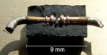

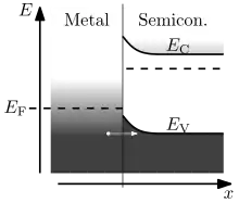
A Schottky barrier, named after Walter H. Schottky, is a potential energy barrier for electrons formed at a metal–semiconductor junction. Schottky barriers have rectifying characteristics, suitable for use as a diode. One of the primary characteristics of a Schottky barrier is the Schottky barrier height, denoted by ΦB (see figure). The value of ΦB depends on the combination of metal and semiconductor.[1][2]
Not all metal–semiconductor junctions form a rectifying Schottky barrier; a metal–semiconductor junction that conducts current in both directions without rectification, perhaps due to its Schottky barrier being too low, is called an ohmic contact.
Physics of formation
When a metal is put in direct contact with a semiconductor, a so called Schottky barrier can be formed, leading to a rectifying behavior of the electrical contact. This happens both when the semiconductor is n-type and its work function is smaller than the work function of the metal, and when the semiconductor is p-type and the opposite relation between work functions holds.[3]
At the basis of the description of the Schottky barrier formation through the band diagram formalism, there are three main assumptions:[4]
- The contact between the metal and the semiconductor must be intimate and without the presence of any other material layer (such as an oxide).
- No interdiffusion of the metal and the semiconductor is taken into account.
- There are no impurities at the interface between the two materials.
To a first approximation, the barrier between a metal and a semiconductor is predicted by the Schottky–Mott rule to be proportional to the difference of the metal-vacuum work function and the semiconductor-vacuum electron affinity. For an isolated metal, the work function is defined as the difference between its vacuum energy (i.e. the minimum energy that an electron must possess to completely free itself from the material) and the Fermi energy , and it is an invariant property of the specified metal:
On the other hand, the work function of a semiconductor is defined as:
Where is the electron affinity (i.e. the difference between the vacuum energy and the energy level of the conduction band). It is valuable to describe the work function of the semiconductor in terms of its electron affinity since this last one is an invariant fundamental property of the semiconductor, while the difference between the conduction band and the Fermi energy depends on the doping.
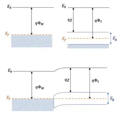
When the two isolated materials are put into intimate contact, the equalization of the Fermi levels brings to the movement of charge from one material to the other, depending on the values of the work functions. This leads to the creation of an energy barrier, since at the interface between the materials some charge get collected. For electrons, the barrier height can be easily calculated as the difference between the metal work function and the electron affinity of the semiconductor:
While the barrier height for holes is equal to the difference between the energy gap of the semiconductor and the energy barrier for electrons:
In reality, what can happen is that charged interface states can pin the Fermi level at a certain energy value no matter the work function values, influencing the barrier height for both carriers. This is due to the fact that the chemical termination of the semiconductor crystal against a metal creates electron states within its band gap. The nature of these metal-induced gap states and their occupation by electrons tends to pin the center of the band gap to the Fermi level, an effect known as Fermi level pinning. Thus the heights of the Schottky barriers in metal–semiconductor contacts often show little dependence on the value of the semiconductor or metal work functions, in strong contrast to the Schottky–Mott rule.[5] Different semiconductors exhibit this Fermi level pinning to different degrees, but a technological consequence is that ohmic contacts are usually difficult to form in important semiconductors such as silicon and gallium arsenide. Non-ohmic contacts present a parasitic resistance to current flow that consumes energy and lowers device performance.
Rectifying properties
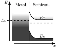
In a rectifying Schottky barrier, the barrier is high enough that there is a depletion region in the semiconductor, near the interface. This gives the barrier a high resistance when small voltage biases are applied to it. Under large voltage bias, the electric current flowing through the barrier is essentially governed by the laws of thermionic emission, combined with the fact that the Schottky barrier is fixed relative to the metal's Fermi level.[6]
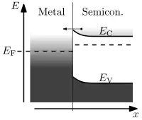
- Under forward bias, there are many thermally excited electrons in the semiconductor that are able to pass over the barrier. The passage of these electrons over the barrier (without any electrons coming back) corresponds to a current in the opposite direction. The current rises very rapidly with bias, however at high biases the series resistance of the semiconductor can start to limit the current.
- Under reverse bias, there is a small leakage current as some thermally excited electrons in the metal have enough energy to surmount the barrier. To first approximation this current should be constant (as in the Shockley diode equation); however, current rises gradually with reverse bias due to a weak barrier lowering (similar to the vacuum Schottky effect). At very high biases, the depletion region breaks down.
Note: the discussion above is for a Schottky barrier to an n-type semiconductor; similar considerations apply for a p-type semiconductor.
The current-voltage relationship is qualitatively the same as with a p-n junction, however the physical process is somewhat different.[7]
Conduction values
The thermionic emission can be formulated as following:
While the tunneling current density can be expressed, for a triangular shaped barrier (considering WKB approximation) as:
From both formulae it is clear that the current contributions are related to the barrier height for both electrons and holes. If a symmetric current profile for both n and p carriers is then needed, the barrier height must be ideally identical for electrons and holes.
Minority carrier injection
For very high Schottky barriers where ΦB is a significant fraction of the band gap of the semiconductor, the forward bias current may instead be carried "underneath" the Schottky barrier, as minority carriers in the semiconductor.[8]
An example of this is seen in the Point-contact transistor.
Devices
A Schottky diode is a single metal–semiconductor junction, used for its rectifying properties. Schottky diodes are often the most suitable kind of diode when a low forward voltage drop is desired, such as in a high efficiency DC power supply. Also, because of their majority-carrier conduction mechanism, Schottky diodes can achieve greater switching speeds than p–n junction diodes, making them appropriate to rectify high-frequency signals.
Introducing a second semiconductor/metal interface and a gate stack overlapping both junctions, one can obtain a Schottky barrier field effect transistor (SB-FET). The gate steers the carrier injection inside the channel modulating the band bending at the interface, and thus the resistance of the Schottky barriers. Generally the most significantly resistive path for the current is represented by the Schottky barriers, and so the channel itself does not contribute significantly to the conduction when the transistor is turned on. This kind of device has an ambipolar behavior since when a positive voltage is applied to both junctions, their band diagram is bent downwards enabling an electron current from source to drain (the presence of a voltage is always implied) due to direct tunneling. In the opposite case of a negative voltage applied to both junctions the band diagram is bent upwards and holes can be injected and flow from the drain to the source. Setting the gate voltage to 0 V suppresses the tunneling current and enables only a lower current due to thermionic events. One of the main limitations of such a device is strongly related to the presence of this current that makes it difficult to properly switch it off. A clear advantage of such a device is that there is no need for channel doping and expensive technological steps like ion implantation and high temperature annealings can be avoided, keeping the thermal budget low. However the band bending due to the voltage difference between drain and gate often injects enough carriers to make impossible a proper switch off of the device. Also, low on-currents due to the intrinsic resistance of the Schottky contacts are typical of this kind of device just like a very hard and unreliable scalability due to the difficult control of the junction area.

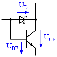
A bipolar junction transistor with a Schottky barrier between the base and the collector is known as a Schottky transistor. Because the junction voltage of the Schottky barrier is small, the transistor is prevented from saturating, which improves the speed when used as a switch. This is the basis for the Schottky and Advanced Schottky TTL families, as well as their low power variants.
A MESFET or metal–semiconductor FET uses a reverse-biased Schottky barrier to provide a depletion region that pinches off a conducting channel buried inside the semiconductor (similar to the JFET where instead a p–n junction provides the depletion region). A variant of this device is the high-electron-mobility transistor (HEMT), which also utilizes a heterojunction to provide a device with extremely high conductance.
A Schottky barrier carbon nanotube FET uses the non-ideal contact between a metal and a carbon nanotube to form a Schottky barrier that can be used to make extremely small Schottky diodes, transistors, and similar electronic devices with unique mechanical and electronic properties.
Schottky barriers can also be used to characterize a semiconductor. In the depletion region of the Schottky barrier, dopants remain ionized and give rise to a "space charge" which in turn give rise to a capacitance of the junction. The metal–semiconductor interface and the opposite boundary of the depleted area act like two capacitor plates, with the depletion region acting as a dielectric. By applying a voltage to the junction it is possible to vary the depletion width and vary the capacitance, used in capacitance voltage profiling. By analyzing the speed at which the capacitance responds to changes in voltage, it is possible to obtain information about dopants and other defects, a technique known as deep-level transient spectroscopy.
See also
References
- ↑ Tung, Raymond T. (2014). "The physics and chemistry of the Schottky barrier height". Applied Physics Reviews. 1 (1): 011304. Bibcode:2014ApPRv...1a1304T. doi:10.1063/1.4858400. ISSN 1931-9401.
- ↑ Schottky barrier tutorial. See also metal–semiconductor junction.
- ↑ Muller, Richard S.; Kamins, Theodore I. (2003). Device Electronics for Integrated Devices (3rd ed.). Wiley. p. 170. ISBN 9780471428770.
- ↑ Sze, S. M. Ng, Kwok K. (2007). Physics of semiconductor devices. John Wiley & Sons. p. 135. ISBN 978-0-471-14323-9. OCLC 488586029.
{{cite book}}: CS1 maint: multiple names: authors list (link) - ↑ "Barrier Height Correlations and Systematics".
- ↑ This interpretation is due to Hans Bethe, after the incorrect theory of Schottky, see Sah, Chih-Tang (1991). Fundamentals of Solid-State Electronics. World Scientific. ISBN 978-9810206376.
- ↑ Balkanski, M.; Wallis, R.F. (2000). Semiconductor Physics and Applications. Oxford University Press. ISBN 978-0198517405.
- ↑ Scharfetter, D. L. (1965). "Minority carrier injection and charge storage in epitaxial Schottky barrier diodes". Solid-State Electronics. 8 (3): 299–311. Bibcode:1965SSEle...8..299S. doi:10.1016/0038-1101(65)90146-2.