| Invented | William Shockley |
|---|---|
| Pin configuration | Anode and Cathode |
| Electronic symbol | |
 | |

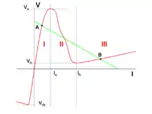
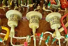
The Shockley diode (named after physicist William Shockley) is a four-layer semiconductor diode, which was one of the first semiconductor devices invented. It is a PNPN diode with alternating layers of P-type and N-type material. It is equivalent to a thyristor with a disconnected gate. Shockley diodes were manufactured and marketed by Shockley Semiconductor Laboratory in the late 1950s. The Shockley diode has a negative resistance characteristic.[1] It was largely superseded by the diac.
Working

Unlike other semiconductor diodes, the Shockley diode has more than one PN junction. The construction includes four sections of semiconductors placed alternately between the anode and cathode in the pattern of PNPN. Though it has multiple junctions, it is termed a diode for being a two-terminal device.
The Shockley diode remains in an OFF state, with a very high resistance, until a voltage greater than the trigger voltage is applied across its terminals. When the voltage exceeds the trigger value, the resistance drops to an extremely low value and the device switches ON. The constituent transistors help in maintaining the ON and OFF states. Since the construction resembles a pair of interconnected bipolar transistors, one PNP and other NPN, neither transistor can turn ON until the other is turned ON due to the absence of any current through the base-emitter junction. Once sufficient voltage is applied and one of the transistors breaks down, it starts conducting and allows base current to flow through the other transistor, resulting in saturation of both the transistors, keeping both in ON state.
On reducing the voltage to a sufficiently low level, the current flowing becomes insufficient to maintain the transistor bias. Due to insufficient current, one of the transistors will cut off, interrupting the base current to the other transistor, hence sealing both transistors in the OFF state.
Usages
Common applications:
- Trigger switch for silicon controlled rectifier
- Relaxation oscillator / sawtooth oscillator
Niche applications:
Typical values

| Description | Range[4] | Typically |
|---|---|---|
| Forward operation | ||
| Switching voltage Vs | 10 V to 250 V | 50 V ± 4 V |
| Holding voltage Vh | 0.5 V to 2 V | 0.8 V |
| Switching current Is | a few µA to some mA | 120 µA |
| Hold current IH | 1 to 50 mA | 14 to 45 mA |
| Reverse operation | ||
| Reverse current IR | 15 µA | |
| Reverse breakdown voltage Vrb | 10 V to 250 V | 60 V |
Dynistor

Small-signal Shockley diodes are no longer manufactured, but the unidirectional thyristor breakover diode, also known as the dynistor, is a functionally equivalent power device. An early publication about dynistors was published in 1958.[5] In 1988 the first dynistor using silicon carbide was made.[6] Dynistors can be used as switches in micro- and nanosecond power pulse generators.[7]
References
- Michael Riordan and Lillian Hoddeson; Crystal Fire: The Invention of the Transistor and the Birth of the Information Age. New York: Norton (1997) ISBN 0-393-31851-6 pbk.
- ↑ "Transistor Museum Photo Gallery Shockley Diode 4 LayerTransistor". semiconductormuseum.com. Retrieved 2019-04-09.
- ↑ "Transistor Museum Photo Gallery Shockley Diode Transistor 4 Layer". semiconductormuseum.com. Retrieved 2019-04-09.
- ↑ "Just Diodes In Hi-Fi Amplifier". 2007-02-21. Archived from the original on 2007-02-21. Retrieved 2019-04-09.
- ↑ Willfried Schurig (1971), amateurreihe electronica: Kennlinien elektronischer Bauelemente. Teil II: Halbleiter Dioden (in German), Berlin: Deutscher Militärverlag, p. 119
- ↑ Pittman, P. (Spring 1958). The application of the dynistor diode to off-on controllers. 1958 IEEE International Solid-State Circuits Conference. Digest of Technical Papers. Vol. I. pp. 55–56. doi:10.1109/ISSCC.1958.1155602.
- ↑ Chelnokov, V. E.; Vainshtein, S. N.; Levinshtein, M. E.; Dmitriev, V. A. (1988-08-04). "First SiC dynistor". Electronics Letters. 24 (16): 1031–1033. doi:10.1049/el:19880702. ISSN 1350-911X.
- ↑ Aristov, Yu.V.; Grekhov, I.V.; Korotkov, S.V.; Lyublinsky, A.G. (September 22–26, 2008). "Dynistor Switches for Micro- and Nanosecond Power Pulse Generators". Acta Physica Polonica A. Proceedings of the 2nd Euro-Asian Pulsed Power Conference, Vilnius, Lithuania, September 22–26, 2008. 115 (6): 1031–1033. doi:10.12693/APhysPolA.115.1031.
External links
- Shockley diode analysis
- Shockley diode information
- Transistor Diodes, by Shockley himself (Jan. 1960)