 | |
| Type | LGA |
|---|---|
| Contacts | 1356 |
| FSB protocol | Intel QuickPath Interconnect |
| FSB frequency | 1× QuickPath |
| Processors | Sandy Bridge-EN Ivy Bridge-EN |
| Predecessor | LGA 1366, LGA 1567 |
| Successor | LGA 2066, LGA 3647 |
| Memory support | DDR3 |
This article is part of the CPU socket series | |
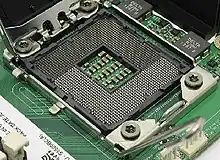
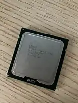
LGA 1356, also called Socket B2, is an Intel microprocessor socket released in Q1 2012 with 1356 Land Grid Array pins. It launched alongside LGA 2011 to replace its predecessor, LGA 1366 (Socket B) and LGA 1567.[1] It's compatible with Intel Sandy Bridge-EN (also known as Romley-EN) and Ivy Bridge-EN microprocessors.
Description
LGA 1356 has 1356 protruding pins to make contact with the pads on the processor. Processors of LGA 1356 and LGA 1366 sockets are not compatible with each other since they have different socket notches.
While LGA 2011 was designed for high-end desktops and high-performance servers, LGA 1356 was designed for the dual-processor and low-end segment of the server market.
It supports 64-bit wide DDR3 triple channel memory, and equipped with 1 Intel QPI connection and 24 PCI Express lanes. Meanwhile LGA 2011 supports quad channel memory, 2 QPI connections and 40 PCIe lanes. Socket LGA 1155, desktop socket of the same generation supports dual channel memory. Each DDR3 channel can support one more DIMM (only applicable to DDR3 and not DDR3-L).[2]
Plans were leaked in early 2011, with estimated releases in the first quarter of 2012.[3] In September 2011, releases were estimated to be at the end of the first quarter of 2012.[4]
Physical design
Socket B2 processors have the following mechanical maximum load limits which should not be exceeded during heatsink assembly, shipping conditions, or standard use. Load above those limits will crack the processor die and make it unusable. The limits are included in the table below.
| Location | Dynamic | Static |
|---|---|---|
| IHS Surface | 890 N (200 lbf) | 266 N (60 lbf) |
Processors using this socket have the same static load limit as previous models using LGA 1366 (Socket B).[5]
Compatible processors
Sandy Bridge-EN
| Socket | Model | Cores
(threads) |
L3Cache | CPU clock rate | Interface | Supported
memory |
TDP | Release
date |
Price
(USD) | ||
|---|---|---|---|---|---|---|---|---|---|---|---|
| Standard | Turbo | ||||||||||
| LGA 1356
Dual Socket |
Xeon E5 | 2470 v2 | 10 (20) | 25MB | 2.4GHz | 3.2GHz | 1× QPI
24× PCI-E 3.0 |
3× DDR3-1600 | 95W | Q1 2014 | $1440 |
| 2470 | 8 (16) | 20MB | 2.3GHz | 3.1GHz | May 14, 2012 | ||||||
| 2450 | 2.1GHz | 2.9GHz | $1106 | ||||||||
| 2450L | 1.8GHz | 2.3GHz | 70W | ||||||||
| 2450Lv2 | 10 (20) | 25MB | 1.7GHz | 2.1GHz | 60W | Q1 2014 | $1219 | ||||
| 2448L | 8 (16) | 20MB | 1.8GHz | 2.1GHz | 70W | May 14, 2012 | $1151 | ||||
| 2449L | 1.4GHz | 1.8GHz | 50W | OEM | |||||||
| 2440 | 6 (12) | 15MB | 2.4GHz | 2.9GHz | 3× DDR3-1333 | 95W | $834 | ||||
| 2430 | 2.2GHz | 2.7GHz | $551 | ||||||||
| 2420 | 1.9GHz | 2.4GHz | $388 | ||||||||
| 2430L | 2.0GHz | 2.5GHz | 60W | $662 | |||||||
| 2428L | 1.8GHz | 2.0GHz | $628 | ||||||||
| 2418L | 4 (8) | 10MB | 2.0GHz | 2.1GHz | 50W | $387 | |||||
| 2407 | 4 (4) | 2.2GHz | N/A | 3× DDR3-1066 | 80W | $250 | |||||
| 2403 | 1.8GHz | $192 | |||||||||
| LGA 1356 | 1428L | 6 (12) | 15MB | 1.8GHz | 3× DDR3-1333 | 60W | $395 | ||||
| 1410 | 4 (8) | 10MB | 2.8GHz | 3.2GHz | 80W | N/A | |||||
| Pentium | 1407 | 2 (2) | 5MB | 2.8GHz | N/A | 3× DDR3-1066 | |||||
| 1403 | 2.6GHz | ||||||||||
| 1405 | 1.2GHz | 1.8GHz | 40W | 2012-08 | $143 | ||||||
Ivy Bridge-EN
See also
References
- ↑ Real World Technologies (September 25, 2010). "Real World Technologies - Intel's Sandy Bridge Microarchitecture". Realworldtech.com. Retrieved August 22, 2011.
- ↑ Hiroshige Goto (April 9, 2010). "Sandy Bridge Interface" (PDF). PC Watch website. Archived from the original (PDF) on September 28, 2011. Retrieved November 12, 2011.
- ↑ Gennadiy Shvets (February 8, 2011). "Details on Intel Xeon E5 product families". CPU World news. Retrieved November 12, 2011.
- ↑ Theo Valich (September 9, 2011). "Intel Romley Delayed to End of Q1 2012? Chipset, CPU Issues Cited". Bright side of news. Retrieved November 12, 2011.
- ↑ page 30. From "Intel® Xeon® Processor E5-2400 Product Family Thermal/Mechanical Design Guide" by Intel

.jpg.webp)