Walter-Schottky-Institut | |
| Abbreviation | WSI |
|---|---|
| Established | 1986 |
| Location |
|
| Field | Semiconductor physics |
Parent organization | Technical University of Munich |
| Website | wsi.tum.de |
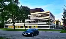
The Walter Schottky Institute (WSI) (German: Walter-Schottky-Institut) is a research center at the Technical University of Munich, dedicated to the physics of semiconductors. Established in 1988, it is located on its Garching campus. It is named after physicist Walter H. Schottky.
History
The idea for an interdisciplinary research facility that would bridge the gap between fundamental physics and applied semiconductor electronics emerged in the early 1980s. In February 1985, Gerhard Abstreiter, professor at the Technical University of Munich, wrote a memorandum about the establishment of a research institute, with specific focus on semiconductor research and device development. After Klaus von Klitzing, who had been working at the physics department of the TU Munich until shortly before the announcement, was awarded the Nobel Prize in Physics in 1985, the idea, which was already supported by the research board of Siemens, received great approval.[1]
Thus, as early as December 1985, the general conditions for founding the research institute as a collaborative project between the Technical University of Munich and Siemens were discussed with Bavarian state government. The construction costs were paid jointly by Siemens and the Bavarian state. After two years of construction, the Walter Schottky Institute was officially inaugurated on 14 July 1988. The university took over the institute completely in 1992.[1]
Facilities

The institute building covers an area of 2400 m2 and provides space for laboratories and offices of eight research groups in four chairs with a total of over 150 employees. Of this, 250 m2 is available as a cleanroom. The equipment includes several molecular-beam epitaxy systems, which are used to fabricate nanoelectronic structures. The institute is considered one of the world's leading research facilities for the fabrication and characterization of semiconductor heterostructures.
In July 2010, an extension building, the Center for Nanotechnology and Nanoscience, was opened in the immediate vicinity.[2]
References
- 1 2 "History of WSI". Walter Schottky Institute. Retrieved 8 January 2021.
- ↑ "Eröffnung des Zentrums für Nanotechnologie und Nanomaterialien: Neues Zentrum für die Nanowissenschaft". Technical University of Munich (in German). 19 July 2010. Retrieved 9 January 2021.